Passive components—resistors, capacitors, and inductors—look deceptively simple on a schematic. Yet every analog circuit is built on the way these three elements enforce conservation laws and store or dissipate energy. This post takes a physics-forward route into passives: starting from charge flow and electromagnetic work, we motivate Kirchhoff’s current and voltage laws, connect them to Ohm’s law, and build intuition for why “voltage drops” and “current continuity” are more than rules-of-thumb.
From there we move into what makes circuits dynamic. Capacitors and inductors introduce energy stored in electric and magnetic fields—so even the simplest RC or LC connection becomes a differential equation. We’ll use that ODE viewpoint to explain transient behavior (charging, discharging, damping), then switch perspectives to the frequency domain where the same circuits become low-pass filters, high-pass filters, and resonators. Along the way we’ll interpret time constants, \(3 dB \) points, phase shifts, and Q factor as different faces of the same underlying physics.
By the end, you should be able to look at a passive network and predict—without memorizing formulas—what it will do to a signal in time and in frequency, and why.
1. Resistor Circuit
Current law
In electronics, we are dealing with the flow of a fundmanetal particle known as electron. These electrons carry a physical quantity measured in \(C\) Coulomb. Charges flowing through a area per unit time is defined as current \(I = \frac{dQ}{dt} = \int{J da} \) measured in \(A\) Ampere, where \(J\) is the current density and \(da\) is the infinitesmal area.
The flow of current must follow the Equation of Continuity, which states that the net amount of charge flowing from a given volume must lead to the change of charge density in that volume:
$$ \oint{J da} = \int{\frac{\partial \rho}{\partial t} dV} $$
which is equation of continuity in integral form. Applying Stokes’ theorem, we obtain the equation of continuity in differential form:
$$ \int{\nabla \cdot J dV} = \int{\frac{\partial \rho}{\partial t} dV} $$
$$ \nabla \cdot J = \frac{\partial \rho}{\partial t} $$
When designing the system, we wish the state of the system to be time-independent \(\partial \rho / \partial t = 0\). Hence, in the transient state, the net flow of current is zero:
$$ \nabla \cdot I = \int{\nabla \cdot J da } = 0 $$
In a circuitry, we working with network of components with inter-connecting nodes. Applying this to each node, then the net-flow of current into and out of the node must be zero.
$$ \sum_{i}{I} = 0$$
which is known as the Kichroff’s current law.
Voltage law
The motion of charge is determined by the electric field and the magnetic field. And it is given from the Lorent’s law of motion:
$$ F = q(E + v \times B)$$
The electric fields \(E\) and magnetic field \(B\) in terms of scalar potential \(V\) and vector potential \(A\):
$$ E = \frac{1}{c}\frac{\partial A}{\partial t} - \nabla V $$
$$ B = \nabla \times A $$
The work done by the field from point b to point a:
$$ W_{ba}=\int_{b}^{a}{F \cdot dr} = q\left(\int_{b}^{a}{E\cdot dr} + \int_{b}^{a}{(v\times B)\cdot dr}\right)$$
Since the second term on the right hand side is perpendicular to the path traveled, the dot product vanishes. And substitute \(E\) into the equation:
$$ W_{ba} = -qV_{ba} + \frac{q}{c}\int_{b}^{a}{\frac{\partial A}{\partial t}} \cdot dr $$
which represents the work done on the charge by the electric field. The first term is straightforward: a charge gain energy from the potential difference \(V_{ba}\) from \(a\) to \(b\). The second term is related to the change of magnetic flux \(\Phi = B \cdot A\). To see this, first assume it is a closed-loop integral \(a = b\) which the potential difference \(V\) vanishes.
$$ W_{closed} = \frac{q}{c} \frac{\partial }{\partial t}\oint{ A \cdot dr} = \frac{q}{c} \frac{\partial }{\partial t}\int{ \nabla \times A \cdot da}$$
$$ W_{closed} = \frac{q}{c} \frac{\partial \Phi}{\partial t} $$
Hence, a charge also gains energy moving in a closed loop from a change of magnetic flux. The contribution from the magnetic field is significantly smaller because it is scaled down by the speed of light \(c = 3\times 10^{8} ms^{-1}\).
In static magnetic field, where there is no change of flux, the work done is now simplified to:
$$ W_{ba} = -qV_{ba} = -q(V_{b} - V_{a}) $$
When that applies to circuitry, we can identify two nodes in the circuit, then the work done on the charge will be characterized by the voltage difference across these components. Furthermore, if we studying a circuit of a closed loop:
$$ \sum_{i}{V_{i}} = 0$$
which states that the net voltage-drop around a circuit loop must be zero.
Relation between voltage and current
To characterize how electronics modify the signal, we study how does the energy carried by the charge being modified across the compoenent. This can be done by taking time derivative on the work done by the field from point \(a\) to point \(b\).
$$ \frac{d W_{ab}}{dt} = \frac{d}{dt}(qV_{ab}) $$
The potential difference \(V_{ab}\) is determined by the spatial distribution of charges within the region. In designing a stable system, we are generally interested in the transient behavior of the system: the system’s microscopic interaction happen in a much smaller time-scale that the system’s observables will be stablized immediately. In this case, the charges will equilibrate so fast that their configuration will become stable immediately and leading to a constant voltage difference across the component.
$$ \frac{dW_{ab}}{dt} = \frac{dq}{dt}V_{ab} = I V_{ab}$$
which says that the if a current is flowing through a potential difference of \(V_{ba}\), there is a dissipation of energy across the component. Or in other words, a electronics component modifies the signal by changing the energy carried by the charge. And this can be measured from the current flow, the voltage difference and the relation between the two.
Conductor
A conductor, in a simple definition, is a type of material that allows for free movement of electrons. It contains a “sea” of electrons that constantly interacting and react instantly to the external field, such that it equilibrate to a stable configuration at a time-scale of \(t< 10^{-12}\). We can then make the assumption that there is no motion of charge within the conductor and hence no electric field within the conductor:
$$ E_{inside} = 0 $$
From the Maxwell’s equation we have:
$$ \int_{V}{(\nabla \cdot E_{inside})dV}= \int_{V}{\frac{\rho}{ \epsilon_{0}}dV} = \frac{Q_{enclosed}}{\epsilon_{0}} = 0 $$
The charge does not live inside the conductor but it resides on the surface of the conductor.
If we do a closed line-integral just right above the surface, so that the perpendicular component approach zero, we have:
$$ \oint_{P}{E\cdot dr} = E_{||} d + E_{inside} d = 0$$
where \(E_{||}\) represents the parallel Electric field just above the surface. Writing it as potential connecting one point to another point of the conductor:
$$ \int_{a}^{b}{ E_{||} \cdot dr} = -(V_{b} - V_{a}) = 0 $$
Here we arrived at a important result of conductor: the conductor surface is at a equal potential. From our previous discussion, the change of energy across a component is characterized by product of the voltage difference and current. Hence, for current flowing through a conductor, there is no change of energy which preserves the integrity of the signal.
Ohm’s law
In non-conductive materials, they usually do not have the sea of electron to provide the charge mobility. The flowing electrons might bump into the material’s atoms and create friction that dissipates energy while transporting. Ohm’s states that eventually it will reach a transient state where a potential difference create a constant flow of electron, meaning the current is proportional to the potential differences:
$$ V \propto I $$
The proportionality constant is called resistance \(R\) measued in ohms \(\Omega \). This gives Ohm’s law:
$$ V = IR $$
The power dissipation across a components for a Ohmic material is then:
$$ P = VI = I^{2}R = \frac{V^{2}}{R}$$
Thevenin’s theorem
Suppose we have two system blocks, each with its input and output. When we connect the output of the first system to the input of the second system, both systems interact and the signal and power transfer changes accordingly.
Thevenin’s theorem states that any two system blocks of resistors could be simplified as a source voltage, source resistance and load resistance. This generalizes to any single input and single output resistor network.
To find the Thevenin equivalent voltage and Thevenin equivalent resistance can be calculated as such:
If nothing is connected to the output, then \(V_{out} = V_{th}\)
(a) If the output is short-circuited, then \(V_{out} = 0\) and \(V_{th} = R_{th} I_{short}\)
Alternatively, Thevenin equivalent resistance can also be computed as such:
- (b) Replace all EMF by short, and computes the equivalent resistance at the output.
- Potential Divider: Voltage signal and Power distribution Considerations
A simpliest example would be a potential divider. If two resistors are treated as two separate systems that connect in series, the potential difference distribute to each of the resistor by the ratio of the resistance.
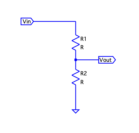
A potential divider circuit
To illustrate, we know the current running through them will be the same. And the voltage drop across \(R_{1}\) and \(R_{2}\) will be the current times each resistance value. The output voltage across \(R_{2}\) will then be:
$$ V_{out} = V_{in} \frac{R_{2}}{R_{1} + R_{2}} $$
Provided if \(R_{2} \gg R_{1}\), \(V_{out} = V_{in}\); there is no loss in signal but realistically signal will experience reduce in magnitude when passing from stages to stages. This is known as the loading effect.
In some other scenario, in communication system or power distribution system, it is of much greater interest to deliver the maximum power than to preserve the voltage signal. Using a potential divider circuit as an example:
The power distribution across \(R_{1}\) and \(R_{2}\) will then be:
$$ P_{1} = V_{in}^{2} \frac{R_{1}}{(R_{1}+ R_{2})^{2}} $$
$$ P_{2} = I^{2} \frac{R_{2}}{(R_{1}+ R_{2})^{2}} $$
We want the resistance ratio such that the power distributed to the second resistance be maximum.
$$ \frac{d P_{2}}{d R_{2}} = I^{2} \frac{d}{dR_{2}} \left[\frac{R_{2}}{(R_{1}+ R_{2})^{2}}\right] = I^{2} \frac{(R_{1} + R_{2})(R_{1} - R_{2})}{(R_{1} + R_{2})^{4}} = 0$$
The maximizing condition gives \(R_{1} = R_{2}\) for the source to deliver the maximum power to the load.
- Thevenin’s equivalent circuit of potential divider
When working with more than one stages, Thevenin’s theorem comes in handy because it reduces stages into \(V_{Th}\), \(R_{Th}\) and \(R_{load}\). Suppose now we are using the potential divider as a driver, to drive a resistive load \(R_{load}\):
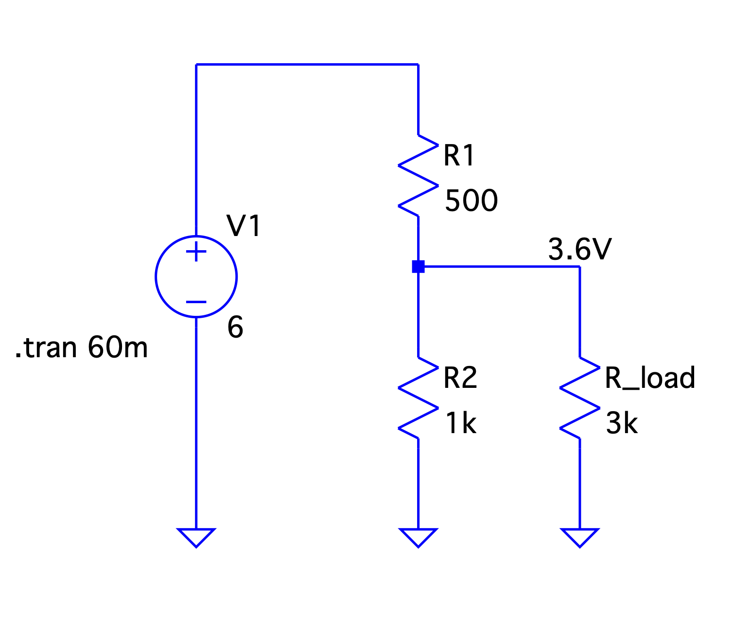
Loading a potential divider circuit. Simulation shows tht the voltage drop across \(R_{load} = 3.6 V\)
The Thevenin’s voltage will be the output voltage as if the node is not connected to any load. $$ V_{Th} = V_{out} = V_{in} \frac{R_{2}}{R_{1} + R_{2}} $$
If \(V_{out}\) is to be shorted, \(V_{out} = 0\) and the short current will be \(V_{in}/ R_{1} = I_{short} = V_{Th} /R_{Th}\). Hence, the Thevenin resistance can be calculated by substituting \(V_{Th}\):
$$ R_{Th} = \frac{V_{Th}}{I_{short}} = \left. \left(V_{in}\frac{R_{2}}{R_{1} + R_{2}}\right) \right/ \left(\frac{V_{in}}{R_{1}}\right) = \frac{R_{1}R_{2}}{R_{1}+ R_{2}} = R_{1}||R_{2}$$
The Thevenin equivalent circuit for the potential divider is then can be drawn as:
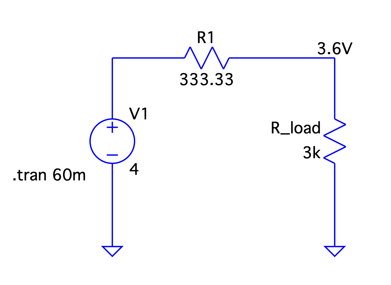
Thevenin equivalent circuit. The simulation result shows 3.6V votlage drop.
The voltage felt at the load can be easily calculated:
$$ V_{out} = V_{Th} \frac{R_{load}}{R_{Th} + R_{load}} = 3.6V $$
which agrees with the simulation value of the potential divider circuit with a reisistive load.
2. RCL circuit
Beside resistive loads, we have two different components that behaves in quite a different manner, the capacitance and inductance; they store energy in the form of electric field and magnetic field. Resistor network allows us to split the power distribution across different loads. Whereas capacitive and inductive loads react to the input signal of different frequencies.
Capacitance
A capacitor is a electronic devices that consists of conducting materials. It store charges in a particular configuration such that the voltage and charge are proportional. The constant of proportionality is called the capacitance.
Let’s solve a simple EM question to illustrate this:
- Flat plate capacitor
The charge resides on the condcutor can be denoted by the charge density multiply by its area. Maxwell’s equation in integral form
$$ \oint_{A}{E\cdot da} = \frac{\sigma A }{\epsilon_{0}} = E \cdot 2A$$ $$ E = \frac{\sigma}{2\epsilon_{0}} $$
For a charge moves from one plate to another, it gain a energy per charge of:
$$ V = \int{E\cdot dr} = E \cdot d = \frac{\sigma d}{2 \epsilon_{0}}$$
Define the capacitance for a flat plate capcitor:
$$ C = \frac{Q}{V} = Q\frac{2\epsilon_{0}}{\sigma d} = QA \left(\frac{2\epsilon_{0}}{A\sigma d}\right) $$
Since the charge density times the area of the plate equals to the total charge stored in the capacitor \(Q = \sigma A\), the capacitance for a particular configuration of conductor is a constant that depends on the geometric of the configuration:
$$ C = 2\frac{\epsilon_{0}A}{d} $$
Capacitance is understood as the ability to store charge in a given potential \(V\). So, it is of no suprise that the \(\epsilon_{0}\), which is material dependent quantity could increase the ability to store charge. As well as increasing the area of the plate, and decreasing the distance of separation between the conducting plates, which reduces the potential difference.
Inductance
- Solenoid with N coils
As for energy stored in the form of magnetic field, consider the Maxwell’s equation:
$$ \nabla \times B = \mu_{0} J + \mu_{0} \epsilon_{0} \frac{\partial E}{\partial t}$$
Casting it in integral form:
$$ \int_{A}{(\nabla \times B ) \cdot da} = \oint_{R}{B \cdot dr } = \mu_{0} I + \mu_{0}\epsilon_{0} \int_{A}{\frac{\partial E}{\partial t} \cdot da}$$
For a single loop of current and static electric, we have the following relationship:
$$ B \cdot 2 \pi r = \mu_{0} I$$
$$ B = \frac{\mu_{0}I}{2\pi r}$$
We are trying to look for how this particular configuration of conductor could have lead to a specific relationship between the voltage and the current. To this end, we need the other Maxwell’s equation as well:
$$ \nabla \times E = -\frac{\partial B}{\partial t}$$
Taking a surface integral of the equation above:
$$ \int_{A}{(\nabla \times E)\cdot da} = \int_{A}{\frac{\partial B}{\partial t}\cdot da}$$
Substitute \(B\) as current:
$$ \int_{A}{\frac{\partial B}{\partial t}\cdot da} = \frac{\mu_{0}}{2\pi} \frac{d}{d t}I \int_{A}{\frac{1}{r}rdrd\theta} = \frac{\mu_{0} r}{2}\frac{d I}{d t}$$
For the term in the left-hand side, we can apply integral theorem to rewrite the surface integral into a closed loop integral:
$$ \int_{A}{(\nabla \times E)\cdot da} = \oint_{R}{E \cdot dr} = V$$
Then, for a single loop of current, we have the following relationship between the voltage and the current:
$$ V = L \frac{dI}{dt} $$
where \(L\), the inductance of a single loop of current, is defined as:
$$L = \frac{\mu_{0}r}{2} $$
For a solenoid with N loops around, the inductant can be generalized to the following:
$$L = \frac{\mu_{0}rN}{2} $$
Physically, the inductance is the ability to resist the change of current by generating a potential difference. The inductance is also a constant that depends on how the current loop is configurated.
Capacitors, inductors and resistor can be connected in series or parallel following the voltage law and current law forming a system block that processes the input signal. Together, they form a linear operator on the input signal. The solution of the output signal accounts to solve a linear ODE.
Linear ODE form by R, C and L
For resistor, capacitor and inductor, the voltage and current relation are listed below:
$$ V = IR $$ $$ V = \frac{Q}{C} = \frac{1}{C}\int{I dt} $$ $$ V = L \frac{dI}{dt}$$
They all relate current and voltage with a time derivative or a integral. To make them more convinent in use we take derivative of every equations.
$$ R\frac{dI}{dt} = \frac{dV}{dt}$$ $$ C \frac{dV}{dt} = I $$ $$ \frac{dV}{dt} = L \frac{d^{2}I}{dt^{2}}$$
In general, we can express the above equation in a general form:
$$ \frac{d^{m}}{dt^{m}}V = k \frac{d^{n}}{dt^{n}}Q$$
We can characterize each components by the number \(d = m-n\). So, resistor, capacitor and inductor has \(d = 0, 1, -1\) respectively.
We want to know what kind of voltage and current dynamics it will cause when we connect them in parallel or series which we will make use of the current and voltage law to formulate the dynamics.
If we connect resistor and capacitor in series, the current running through both components will be the same from the current law.
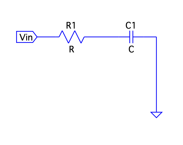
A simple RC circuit connected in series
Hence, we must have
$$ C \frac{dV_{C}}{dt} = I = \frac{V_{R}}{R}$$
$$ \frac{dV_{C}}{dt} = \frac{V_{R}}{RC} $$
where \(V_{C}\) and \(V_{R}\) each denotes the voltage drop across capacitor and resistor respectively. Depending on which node we try to probe the circuit, we can rename the voltage as input voltage and output voltage and hence the RC circuit form a first-order linear differential equation on the voltage.
What if we connect the RC in a parallel fashion?
RC circuit connected in parallel
In this case, the voltage across each component will be the same but current will be divided.
$$ I_{R}R = \frac{1}{C} \int{I_{C} dt}$$
Taking derivative
$$ \frac{dI_{R}}{dt} = \frac{I_{C}}{RC} $$
Connection in series leads to first-order linear ODE in their voltage, whereas connection in parallel leads to first-order linear ODE in their current. This makes sense, because the voltage law implies they have equal current and the current law implies they have equal voltage. RC circuit create a firt order ODE because there is a different in the order of time derivative in their respective physical law. eg. resistor with \(d_{R} = 0\) and capacitor with \(d_{C} = 1\) makeing a difference of \(O_{RC} = d_{R} - d_{C} = 1\) which invitably leads to a first-order ODE.
A more interesting case when we connect inductor to capacitor. \(O_{CL} = 1- (-1) = 2\), which tells us that they will form a second-order ODE.
If connecting them in series,
A CL circuit connected in series
$$ C\frac{d^{2}V_{C}}{dt^{2}} = \frac{dI}{dt} = \frac{V_{L}}{L}$$
$$ \frac{d^{2}V_{C}}{dt^{2}} = \frac{dI}{dt} = \frac{1}{LC}V_{L} $$
If they were connected in parallel:
$$ L \frac{d^{2}I_{L}}{dt^{2}} = \frac{I_{C}}{C}$$
$$ \frac{d^{2}I_{L}}{dt^{2}} = \frac{1}{LC} I_{C}$$
As expected, they lead to a second-order differential equation in either voltage or current. It is also worth noting that the current law will restrict \(I_{L}\) and \(I_{C}\) be opposite sign. This leads to the equation of motion of the form
$$ \frac{d^{2}x}{dt^{2}} = -kx$$
which assembles the equation of motion for a oscillating pendulum with the spring constant replace by \(\frac{1}{CL}\).
Time series analysis
Though we can configure the input and output differently, it will lead to different equation of motion. But for RC connected in series, they will be related by the following equation:
$$ \frac{dV_{C}}{dt} = \frac{V_{R}}{RC}$$
By configuring the input and output voltage accordingly, we will have different dependent of \(V_{in}\) and \(V_{out}\) in place of \(V_{C}\) and \(V_{R}\).
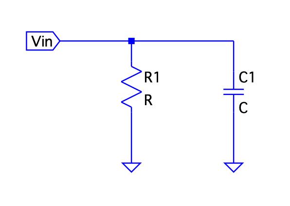
- Case 1: Output voltage across capacitor
A RC circuit conneccted in series with output measured across the capacitor
It must follow that:
$$ V_{C} = V_{out} $$
$$ V_{R} = V_{in} - V_{out}$$
The voltage across the resistor depends on the direction of the current flow.
which leads to the first-order linear ODE:
$$ \frac{dV_{out}}{dt} = \frac{1}{RC} (V_{in} - V_{out}) $$
$$ \frac{d V_{out}(t)}{d t} + \frac{1}{RC} V_{out}(t) = \frac{1}{RC} V_{in}(t) $$
With the source term \(\frac{1}{RC} V_{in}(t)\). Let’s assume for the time being a constant voltage input \(V_{in} = V_{const}\). This equation has a general solution of the form:
$$ V_{out} = V_{homogeneous} + V_{inhomogenous} $$
Treating \(V_{const} = 0\), and solving the ODE with separation method with the initial condition \(V_{out} (t=0) = V_{const}\), we yield the following homogeneous solution:
$$ V_{out}(t) = V_{const} e^{-\frac{t}{RC}}$$
The inhomogeneous case can be solved by integrating factor. For constant source term \(V_{in} = V_{const}\), we have the following solution:
$$ V_{inhomogenous} = V_{const}$$
Introducing the initial condition \(V_{out} (t= 0) = 0\)
$$ V_{out} = V_{const}(1- e^{-\frac{t}{RC}})$$
As we can see in the first case is a exponential decay from \(V_{const}\) and assmytotic to the \(V = 0\). This characterizes the capacitor decay from its charge state to its discharged state. In the second case, the capacitor is initially discharged, with \(V = 0\) and approaching the charge state \(V= V_{const}\).
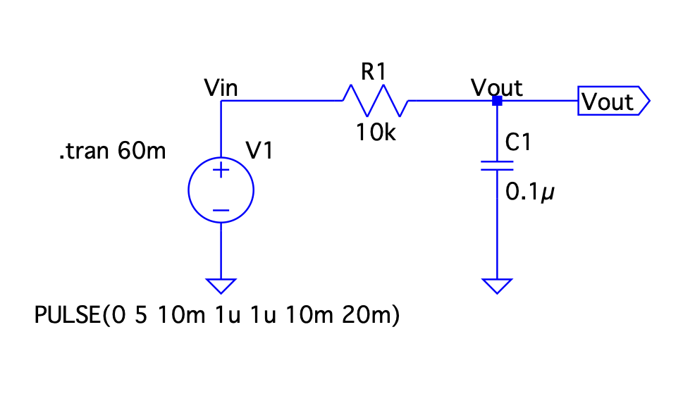
This can be illustrated by simulation with an input voltage of a square wave of \(5V\) with period of \(20ms\).
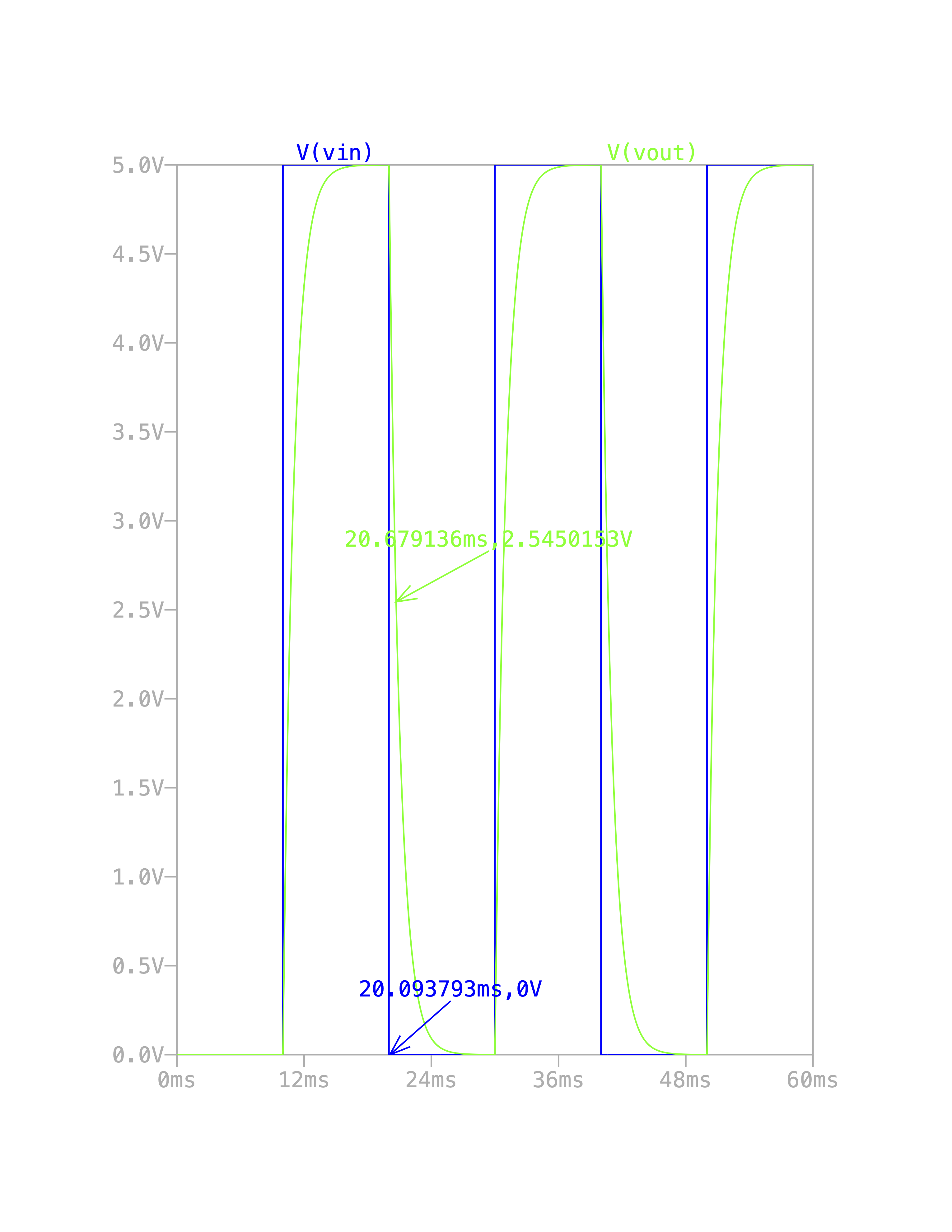
RC circuit simulation with square wave input. It shows both the charging process and the discharging process.
We can observe the rising \(V_{out}\) signal in the region of high \(V_{in}\) region that indicates the capacitor charging. On the low-state of the square wave, the capacitor signal \(V_{out}\) is discharging. To verifies the simulation agrees with the calculation, we take a single point when the output voltage falls to half of its value. This happens at its half-life:
$$ t = RC\ln{2} = 0.69ms $$
From the annotated point on graph, we have \(20.678 - 20.094 = 0.58ms \), with a fractional error of \( \frac{0.69- 0.58}{0.58}= 0.18 \). Not too bad I guess.
The rate of decaying depends on the product of capacitance and resistance, which is commonly defined as the time constant \(\tau = RC\) for the RC circuit. The effect of a larger capacitance meaning slower change of voltage with the same current flow. Thus, leading to a slower charging and discharing time. The present of a resistor is to acts against the flow of current, which in turn has the same effect of slowing down charging rate.
A different perspective on the result is that, the RC circuit with output measures across the capacitor is considered as integrator on the input voltage. This can be eaily shown in the equation as well as on the time series plot. This might come in handy when working with experiment that has a meaningful integral output.
- Case 2: Output Voltage across the Resistor
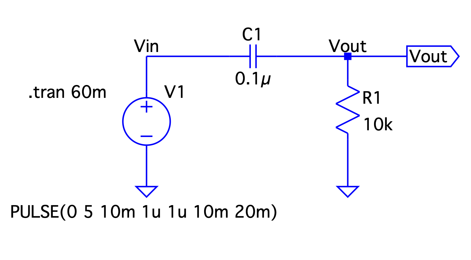
RC circuit connected in series with output measured across the resistor.
$$ V_{R} = V_{out} $$
$$ V_{C} = V_{in} - V_{out}$$
Following the same analysis, this leads to the differential equation
$$ \frac{d}{dt} V_{out} + \frac{1}{RC} V_{out} = \frac{d V_{in}}{dt} $$
It is tempting to treat this question the same way as we did in the previous question. But with the input signal being differentiatied, there are some subtlties to consider.
Supose \(V_{in}\) is a step function that has a jump at \(t_{0}\),
$$ V_{in}(t) = \begin{cases} V_{const} &\text{if } t < t_{0} \\ 0 &\text{if } t > t_{0} \end{cases} $$
There is a discontinuity at \(t_{0}\). Derivative at \(t_{0}\) will be infinite and zero elsewhere. We know one function (or distribution) that does exactly that, the Dirac Delta function:
$$ V_{const}\delta (t - t_{0}) = \left. \frac{dV_{in}}{dt}\right\vert_{t=t_{0}} = \begin{cases} \infty &\text{if } t = t_{0}\\ 0 &\text{if } t \ne t_{0}\end{cases} $$
The equation then becomes:
$$ \frac{d}{dt} V_{out} + \frac{1}{RC} V_{out} = V_{const}\delta (t-t_{0}) $$
The homogeneous solution with integrating factor \(\alpha = e^{t/RC}\)
$$ V_{homogeneous}(t) = V_{0} e^{-\frac{t}{RC}}$$
From the initial condition, \(V_{out}(t= 0) = 0\), so \(V_{0} = 0\); the homogeneous term does not contribute to the solution.
The inhomogeneous solution:
$$ V_{inhomogeneous}(t) = V_{const}e^{-\frac{t}{RC}} \left[\int^{t_{0} - \epsilon}{e^{\frac{t}{RC}}\delta (t-t_{0})dt} + \int_{t_{0}}^{t}{e^{\frac{t}{RC}}\delta (t-t_{0})dt} \right] $$
The non-homogeneous solution separete into integral of two regions. Because of the property of the Dirac Delta function, the only contribution comes from the time region \(t> t_{0}\).
Hence, in the region \(t < t_{0}\), the contribution from both the homogeneous term and inhomogeneous term are zero.
$$ V_{out}(t)\vert_{t< t_{0}} = 0 $$
For the region \(t > t_{0}\),
$$ V_{out}(t)\vert_{t> t_{0}} = V_{const}e^{-\frac{t}{RC}} \int_{t_{0}}^{t}{e^{\frac{t}{RC}}\delta (t-t_{0})dt} = V_{const}e^{-\frac{t-t_{0}}{RC}} $$
At the \(t = t_{0}\), \(V_{out}(t)\) jumps from \(0V\) to \(V_{const}\), which reaches its maximum. After \(t> t_{0}\), \(V_{out}(t) = V_{const} e^{-(t-t_{0})/RC}\), it decays exponentially with the time constant \(RC\).
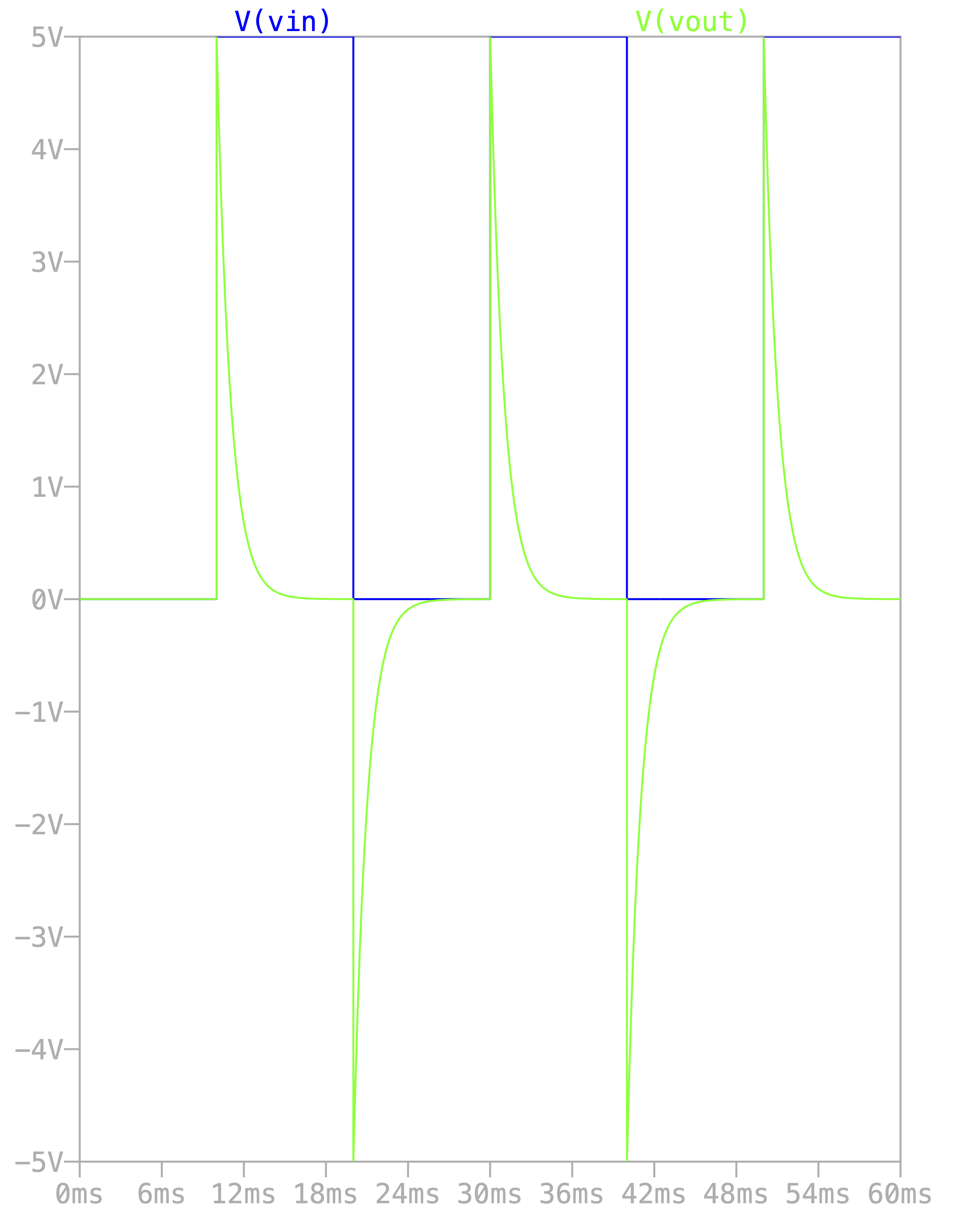
RC circuit with output measured across the resistor. It behaves as a differentiator to the input signal.
The qualitative behavior of the simulation agrees with our analytic predicton. However, at the falling edge, the output voltage becomes negative because the derivative becomes negative at the falling edge.
The sharply peaked behavior of the capacitor is known as a differentiator because it is a derivative on the input voltage. The discussion of differentiator and integrator is important because they process the incoming signal in different manner. eg. For a fast varing signal, the integration of the input signal will not reflect the information as much as a differentiation of the fast varying signal. Whereas a slow varying signal, the differentiator won’t reflect this character as much as an integrator on its output.
- Case 3: RCL parallel resonant circuit
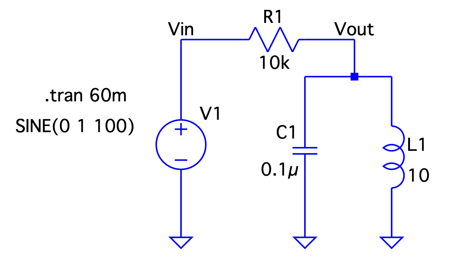
Resistor and capacitor connected parallel to the inductor forming a resonance circuit.
A extension to the CL circuit, we add a resistor parallel to the inductor. This leads to an additional term with a first-order time derivative to the equation.
$$ I_{R} = I_{C} + I_{L}$$
$$ \frac{V_{R}}{R} = C\frac{dV_{C}}{dt} + \frac{1}{L} \int{V_{L}dt} $$
Taking a time derivative on both side:
$$ \frac{1}{R} \frac{dV_{R}}{dt} = C\frac{d^{2}V_{C}}{dt^{2}} + \frac{1}{L}V_{L} $$
From the schematic, we can conclude that:
$$ V_{R} = V_{in} - V_{out} $$
$$ V_{L} = V_{C} = V_{out} $$
which leads to equation:
$$ C\frac{d^{2}}{dt^{2}} V_{out} + \frac{1}{R}\frac{d}{dt} V_{out} + \frac{1}{L} V_{out} = \frac{d}{dt} V_{in}$$
which assembles a second-order linear ODE with restorative force as well as resistive terms.
$$ m\frac{d^{2}x}{dt^{2}} + b \frac{dx}{dt} + kx = F(t)$$
Its dynamics, in addition to that of a oscillating pendulum as in the CL circuit, it also has a damping term. The coefficient of friction that resists the motion, is the coefficient of the first-order derivative. The damping coefficient is defined by \(1/CR\) for this particular circuit configuration and its effect is to dissipates the energy stores in the system. In the absence of the forcing term and suppose the system comes with an initial swing, it will eventually leads to a static state. But in the present of the forcing term, it will stablize in an oscillatory state.
For the above RCL resonant circuit, the resonant frequency is \(f_{0} = 1/(2\pi \sqrt{CL}) = 160Hz\). Running a time series simulation reveal the fact that the static state of the system will be oscillating.
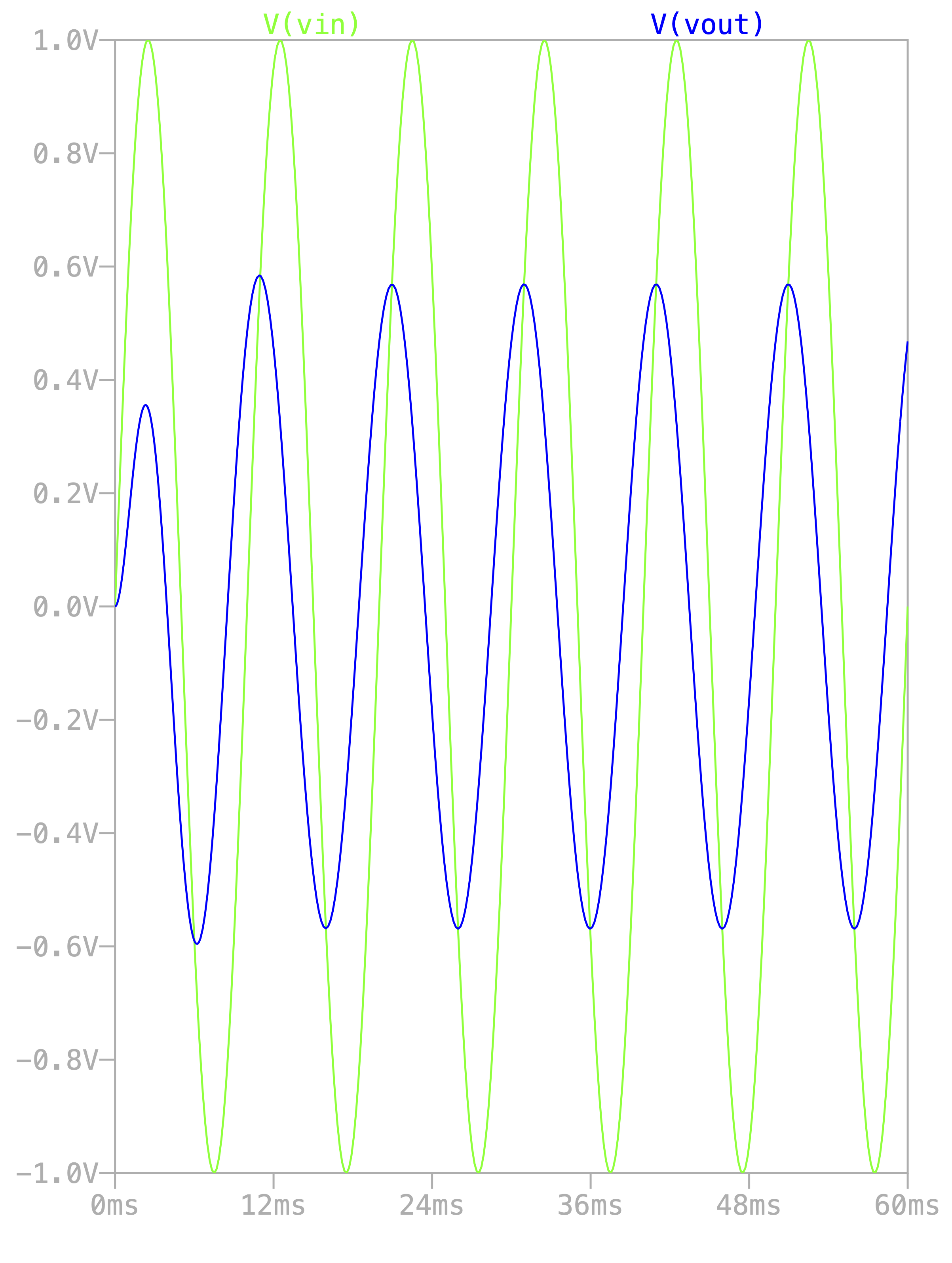
Time series plot of both input and output signal. The output signal shifted in phase and being attenuated.
If we isolate the system itself by assuming zero input voltage and giving it a initial swing, how will the system behave? This is equivalent to solve for the homogeneous equation. The properties of the homogeneous solution of the damped oscillation is instrinsic to the system. In order words, its properties depend on the resistance, capacitant and inductant. Define the terms:
$$ \gamma = \frac{1}{2RC}$$
$$ w_{0} = \frac{1}{CL}$$
The first term is known as the damping coefficient and the second term is known as the natural angular frequency. Rewriting the equation in the homogeneous case:
$$ \frac{d^{2}V}{dt^{2}} + 2\gamma \frac{dV}{dt} + w_{0}^{2} V = 0$$
Assume \(V(t) = V_{0}e^{\lambda t + \phi}\), leading to quadratic equation of the unknown parameter \(\lambda\):
$$ \lambda^{2} + 2\gamma \lambda + w_{0}^{2} \lambda = 0$$
Hence, the roots for the quadratic equation has the solution of
$$ \lambda = \frac{-2\gamma \pm \sqrt{4\gamma^{2} - 4w_{0}^{2}}}{2} = -\gamma \pm \sqrt{\gamma^{2} - w_{0}^{2}} $$
The solution:
$$ V_{out} (t) = V_{0} e^{-\gamma t} e^{\pm t \sqrt{(\gamma^{2} - w_{0}^{2})} }$$
Depending on the relative magnitude of the damping coefficient and the natural angular frequency, the solution can be of these three types of qualitative behaviors:
- Underdamped. \(w_{0} > \gamma \)
The exponent will be complex number which leads to a oscillator behavior with an exponential dampping.
$$ V_{out} = V_{0} e^{-\gamma t} e^{-iw_{d}t + \phi }$$
where we define \(w_{d} = \sqrt{(w_{0}^{2} - \gamma^{2})}\)
- Overdamped. \( \gamma > w_{0} \)
$$ V_{out} = V_{0} e^{-(\gamma+w_{d}) t + \phi} $$
- Critical Damped. \( \gamma = w_{0} \)
$$ V_{out} = V_{0} e^{-\gamma t + \phi}$$
Plotting these different solutions and compare their behavior overtime:
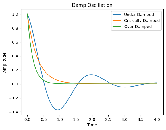
Three types of solution for a damped oscillation.
The three solutions all reach a state of zero amplitude; they differed in how fast they approach this static state. Thus, the effect of the damping coefficient is to resist the motion of the system and to dissipate energy until it is stationary.
In electronic parameter, \(\gamma = 1/RC \), the larger the resistor the more rapidly it dissipates the energy, which makes sense because this is the only component that dissipates energy. The question arises from the fact that capacitance also affect the rate of dissipation. The smaller the capacitance also leads to an increase in rate of dissipation. But physically why?
- Power
To have a quantitative measure of the power dissipation, we need to calculate the average power dissapated. In static case, power is computed as:
$$ P = VI $$
But now we are working with oscillator voltage and current, so the current and voltage in general can be written as:
$$ V(t) = V_{0} \cos{(wt)}$$ $$ I(t) = I_{0} \cos{(wt + \phi)}$$
where \(w\) is the angular frequency and \(\phi\) is the phase difference between the voltage and the current. As we shall see in the transfer function analysis, the difference in phase arises from how we assembles the electronics components, but for the time being, this is reckoned as a fact.
The average power is then calculated by summing the product of voltage and current over its period and divided by the period:
$$ \left< P \right> = \frac{1}{T} V_{0} I_{0} \int^{T}_{0}{\cos{(wt) \cos{(wt+\phi)}}dt}$$
By triogometric identities, the integrand can be simplified to:
$$ \cos(wt)\cos(wt+ \phi) = \cos(wt)[\cos(wt)\cos(\phi) - \sin(wt)\sin(\phi)]$$
$$= \cos^{2}(wt)\cos(\phi) - \frac{1}{2}\sin(2wt)\sin(\phi) $$
Intergrating over its period, the second term vanishes:
$$ \left< P \right> = \frac{1}{T} V_{0}I_{0} \cos(\phi) \int_{0}^{T}{\cos^{2}(wt)dt}$$
$$ \left< P \right> = \frac{1}{2} V_{0}I_{0} \cos(\phi)$$
The average power is also scaled by the phase difference between the voltage and current. This is the reason why the capacitance has the dissipative effect. The capacitor stores energy in terms of electric field by the processing of charging. This in turns lags the voltage from the current, creating the phase difference that actually reduces the dissipation of energy from the resistive load. We will come back to the phase difference dependent on the electronic parameter \(CL\) and the configuration of the circuitry in the next section.
Transfer Function
Assuming input voltage and input current to be complex quantity with a monochromatic angular frequency of \(w\)
$$ \widetilde{V}(t) = V_{0} e^{-iwt} $$
where \(V_{0}\) is the magnitude of the voltage signal.
It is convient to express it in terms of complex number because it will reduce the linear ODE that governs the dynamics of the voltage into an algebraic equations in the complex plane. For example,
$$ \frac{d}{dt} \widetilde{V}(t) = -iw\widetilde{V}(t)$$
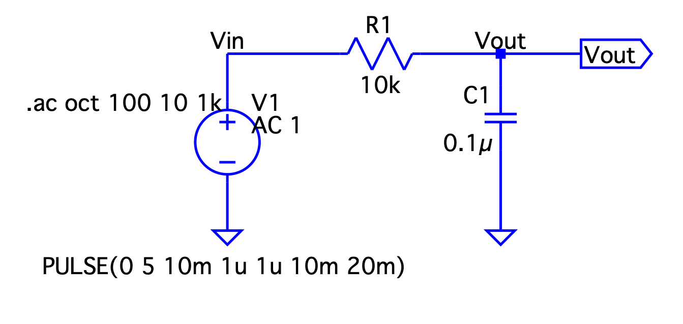
- High-pass filter
Hence, for RC circuit:
A differentiator also behaves as a high-pass filter.
$$ \frac{d}{dt} \widetilde{V_{o}} + \frac{1}{RC}\widetilde{V_{o}} = \frac{d \widetilde{V_{i}}}{dt} $$
$$ \left(-iw + \frac{1}{RC}\right) \widetilde{V_{0}} = -iw \widetilde{V_{i}}$$
Define the transfer function \(T(w)\). It mesures the absolute ratio of the output volage to the input voltage.
$$T(w) = \left| \frac{\widetilde{V_{o}}}{\widetilde{V_{i}}} \right|$$
Notice the transfer function is scalar quantity that measures the relative magnitude between the output signal and the input signal. And more importantly, it has no time dependent but only depends on the frequency. For the RC circuit,
$$ T(w) = \left| \frac{-iw}{-iw + \frac{1}{RC}} \right| = \frac{1}{\sqrt{\left(\frac{1}{wRC}\right)^{2} + 1}} $$
The transfer function for RC circuit with output voltage defined on the resistor has two region of behavior. For low angular frequency, \(w \ll RC\), \(T(w) \ll 1\), meaning it produces low output when the input frequency is lower than the time constant \(\tau = RC\). Whereas in the case of high angular frequency, \(w\gg RC\), the transfer function \(T(w) = 1\), which allows the high frequency signal to go through. Hence, this RC setup is known as the high-pass filter.
- Reactant and Impedence
One simplistic view of the method is redefined capacitance and inductance in the complex plane, which generalizes resistance to impedance. Recognizing:
$$ \frac{d}{dt} \equiv -iw$$
$$ C\frac{d}{dt}\widetilde{V} = -iwC\widetilde{V} = \widetilde{I}$$
Define the reactant \( \widetilde{X} = \widetilde{V}/\widetilde{I} \), we have purely imaginary reactant for capacitor and inductor:
$$ X_{C} = \frac{i}{wC} $$
And similarly for inductance:
$$ X_{L} = -iwL $$
We can further generalize the quantity impedance, which is the sum of resistance and reactant, which composes of both real and imaginary part each representing the resistive part and reactive part of a circuit configuration.
This perspective of loads have the advantage to treat passive circuit with either AC or DC signal in the same way as resistor network. For example, Ohm’s law can be re-expressed as such:
$$ \widetilde{V} = \widetilde{Z}\widetilde{I} $$
- Low-pass filter
For example, consider an integrator where the output voltage is measured across the capacitor.
An integrator behaves as a low-pass filter.
It forms a potential divider with \(R_{1} = R, R_{2} = X_{C}\)
$$ \widetilde{V_{o}} = \widetilde{V_{i}} \frac{X_{C}}{R + X_{C}} = \widetilde{V_{i}} \frac{\frac{i}{wC}}{R + \frac{i}{wC}}$$
$$ T(w) = \left| \frac{i}{wCR +i} \right| = \frac{1}{\sqrt{(wCR)^{2} + 1} }$$
As \(w \gg CR\), \(T(w) \approx 0\) and \(w\ll CR\), \(T(w)\approx 1\). Opposite to the potential measure across the resistor (differentiator), an integrator is a low-pass filter.
- Decibel per Octave
One way to quantify the relative magnitude dependence on the frequency is to define the quantity “decibel per octave”. One octave means a double of frequency. Decible is the measure of the signal power relative to a reference level in logarithmic scale. eg. Each decibel \(dB\) corresponding to \(10 \log{\frac{P}{P_{0}}}\). Because power is proportional to the square of the voltage \(P \propto V^{2}\), we have decibel measure in transfer funti: \(20 \log{\frac{V}{V_{0}}} = 20 \log{T(w)} \).
Plotting the transfer function in dB with the frequency on a octave scale, we can clearly observe the transfer function is at maximum at a small frequency and decreases when frequency drops, which matches our prediction that it is a low-pass filter.
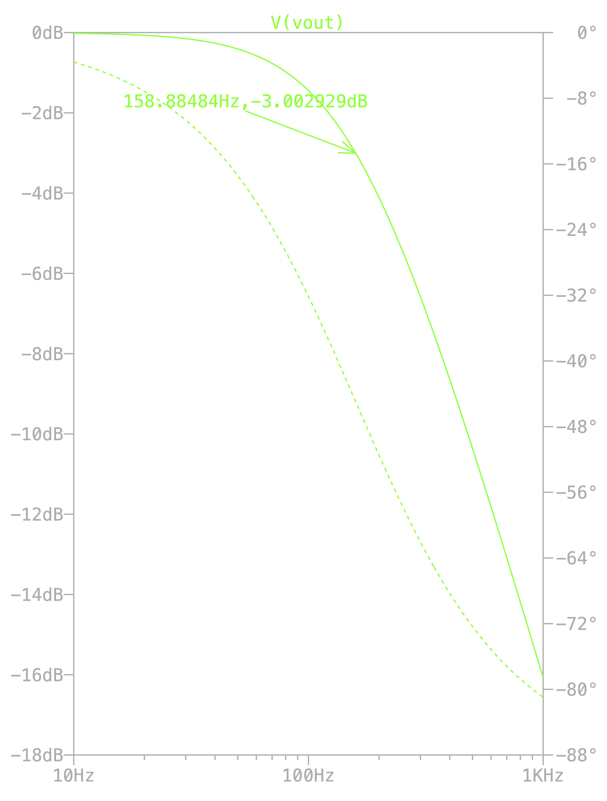
Frequency response of a low-pass filter with its \(3dB\) point labelled.
Diving a little deeper into the high frequency region. At high frequency, the transfer function scales roughly as \(w^{-1}\). This behavior is known as the power-law scaling with coefficient of \(-1\) in phase transition literature. Doubling the frequency in the high frequency region will reduce the amplitude by half. This is shows as a straight line on the plot. In terms of decibel, we can characterize the striaght line by the large frequency behavior of \(w^{-1}\):
$$ 20 \log_{10}{\frac{1}{2}} = -6 dB / octave$$
Whereas in the low frequency region, \(T(w) \approx 1\), which corresponds to a horizontal line on the curve. Separating the two regions of behavior is called the 3dB point. The point is annotated on the graph for the low-pass filter with measured value of \(159 Hz\).
- 3dB point
In the electrical engineering literature, the \(3dB\) point is often being defined by the frequency in which the transfer function becomes \(T(w) = 1/\sqrt{2}\).
$$ \frac{1}{\sqrt{2}} = \frac{1}{\sqrt{(wCR)^{2} + 1}} $$
$$ f_{3dB} = \frac{1}{2\pi CR} = 160Hz$$
As an alternative, we can refer to the phase transition literature and define the \(3dB\) point from the singularity of \(\widetilde{T(w)}\).
$$ \lim_{w\to -i/CR} \widetilde{T(w)} = \lim_{w\to -i/CR} \frac{i}{wCR + i} = \infty$$
The transfer function has a singular point at the \(3dB\) point, which leads to a power-law scaling and a phase transition.
- Phase Shift
As shown on the plot above, it also includes the dotted plot that indiciates the phase difference, showing that the input and output voltage is out of phase. To see this, refer back to the complex transfer function:
$$ \widetilde{T(w)} = \frac{i}{wCR + i} = \frac{1+ iwCR}{1+(wCR)^{2}}$$
For large \(w \gg CR\), the transfer function can be approximated to \(\widetilde{T(w)} \approx \frac{i}{wCR} \), a pure imaginary number. This implies that the output voltage leads the input voltage by \(90^{\circ}\).
In general, for a complex number \(Z = Re(Z)+ iImg(Z) = Ae^{\phi}= A\cos{\phi} + iA\sin{\phi} \). The phase and magnitude can be calculated by matching the real and imaginary part with the Euler representation of complex number.
$$ A = \sqrt{Re(Z)^{2} + Img(Z)^{2}}$$
$$ \phi = \arctan{\frac{Img(Z)}{Re(Z)}}$$
For pure imaginary output, \(\phi = \arctan{\infty} = \pi /2\), which verifies that claim earlier.
- LCR resonant circuit
Considering LCR resonant circuit configured in different ways:
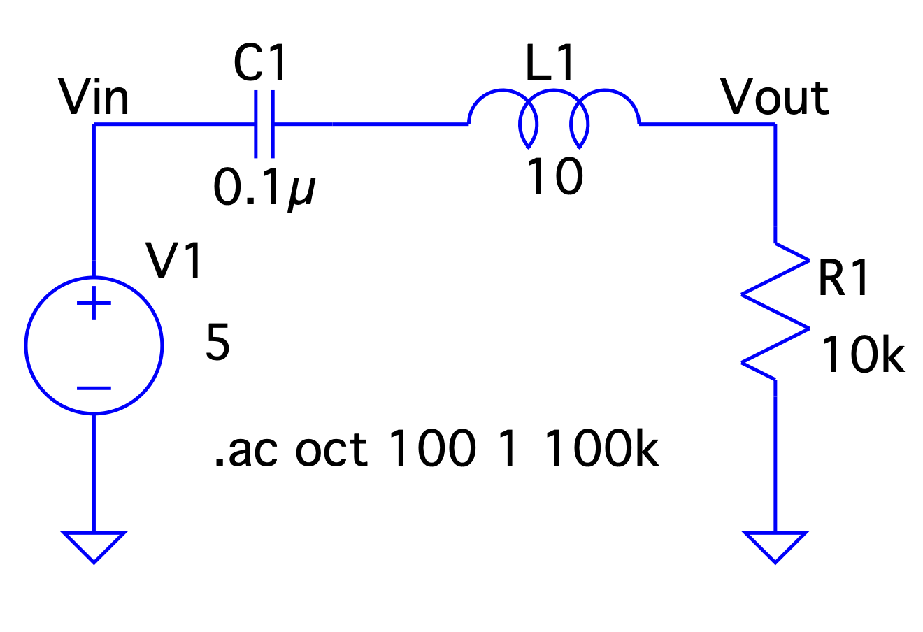
A serially connected RCL circuit with output measured across the resistor.
Because the capacitor and inductance are connected in series, we can calculate their reactant combined.
$$ X_{tot} = X_{C} + X_{L} = \frac{-1}{iwC} -iwL$$
Together with the resistor, they form a potential divided with output voltage measure across the resistor. This leads to the transfer function of the following form:
$$ \widetilde{T(w)} = \frac{R}{X_{tot} + R} = \frac{R}{\frac{-1}{iwC} - iwL + R} = \frac{iwCR}{w^{2} CL + iwCR - 1}$$
Divide nominator and denominator so that the highest power of \(w\) in the denominator is 1. And define the damping coefficient \(\gamma_{0} = \frac{R}{L}\) and the resonant frequency \(w_{o} = \frac{1}{\sqrt{CL}}\).
$$ \widetilde{T(w)} = \frac{iw\frac{R}{L}}{w^{2} - \frac{1}{CL} +iw \frac{R}{L}} = \frac{-iw\gamma_{0}}{w^{2} - w_{0}^{2} +iw \gamma_{0}}$$
$$ |\widetilde{T(w)}| = \frac{w\gamma_{0}}{\sqrt{(w^{2} - w_{o}^{2})^{2} + (w\gamma_{0})^{2}}}$$
When the input frequency reaches the resonant frequency of \(w = w_{0}\) or \(f_{0} = w_{0}/2\pi = 1/(2\pi \sqrt{LC}) = 159Hz\), the transfer function reaches its maximum \(T(w) = 1\) or \(20\log_{10}(1) = 0dB\) in decibel. Moving away from the resonant \(w_{0}\) will increase the factor of the denominator and results in a smaller transfer function. In a sense, the resonant circuit picks up the frequency that is close to the resonant frequency. As can be seen in the figure below:
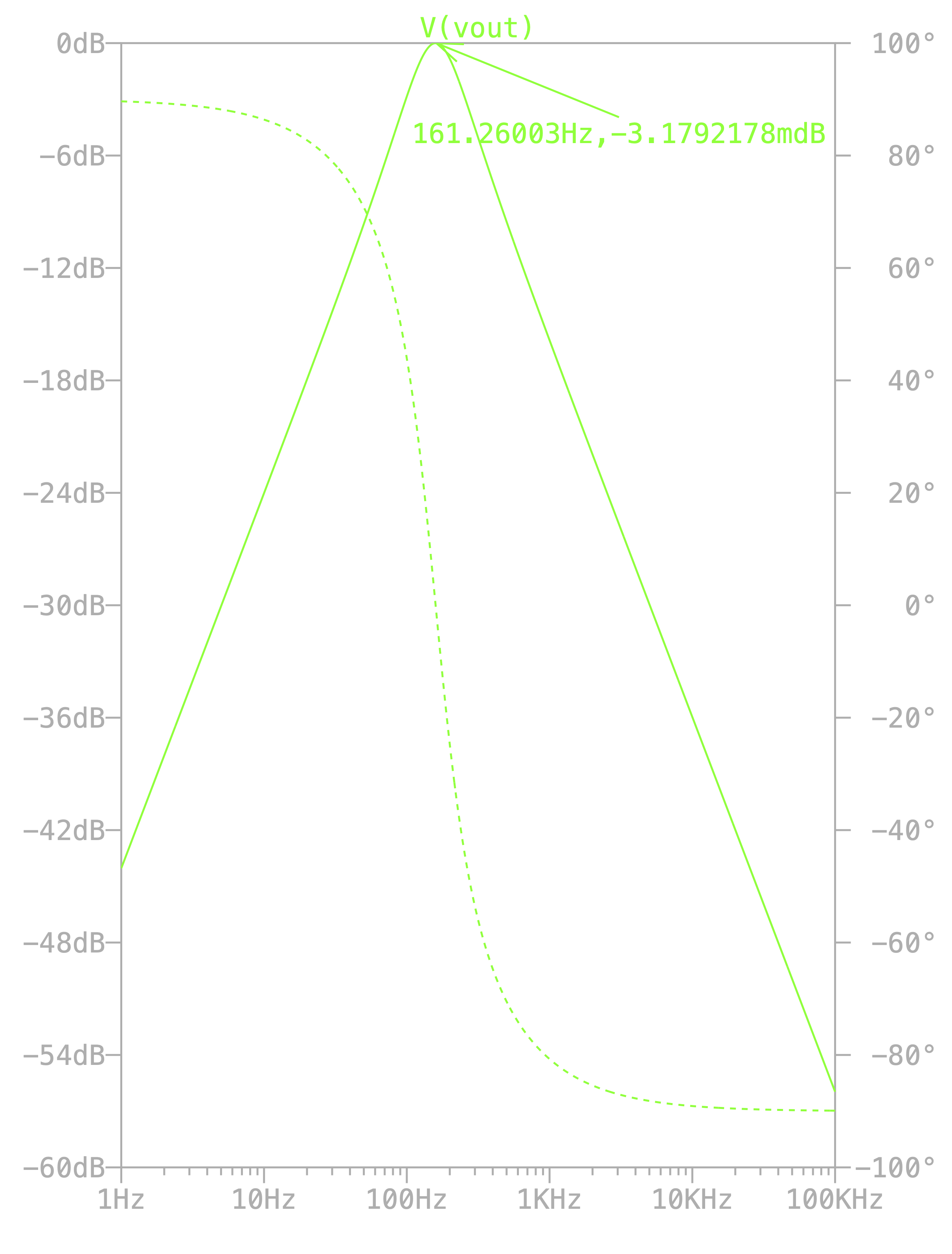
Frequency response of a resonance circuit. It peaks at the resonance frequency.
- Damping coefficient
In the RCL series, the damping coefficient is different from the RCL parallel connection in the time series analysis. Back then, it was define to be \(\gamma = 1/ RC\), comparing with RCL series \(\gamma = R/L \). A series connection form a voltage divider between components. Therefore, the voltage law is applied to connect the voltage between each every components. Writing the voltage in terms of their common current formulates the second-order differential equation in the function of the current. The coefficient of the second-order derivative must be of inductance due to its nature \(L \frac{dI}{dt} = V\). It is the “mass” term of the current second-order ODE. The inductor is a component that slows down the change of current.
Similar conclusion can be made for RCL parallel connection, where it forms a current divider and so on and so forth. The capacitor is a component that slows down the change of voltage due to its nature \(C\frac{dV}{dt} = I\).
To see this from another perspective, we bring back a topic that being postponed in the discussion of phase difference between voltage and current. Recall the average power depends not only on average current and average voltage, but also their relative phase:
$$ \left< P \right> = I_{rms} V_{rms} \cos{\phi}$$
The present of \(C\) and \(L\) in the dissipative term leads us to consider the relation between the relative phase and \(C\) and \(L\). If we generalize Ohm’s law to impedence, which is a complex number in general, we will have the following relationship:
$$ \widetilde{V} = \widetilde{I} \widetilde{Z} $$
Expressing them in Euler form:
$$ V_{0}e^{i\theta} = I_{0}Z_{0} e^{i(\theta + \phi)} $$
Hence, impedance will shift the relative phase between the voltage and current if it contains imaginary part, or for \(\theta_{Z}\) multiple of \(\pi\). To verify that the relative phase \(\phi\) dependence on \(C\) and \(L\), we can calculate their Thevenin’s impedance in the parallel and series case. And evaluate the phase of the imepednace.
For series connection, \(V_{Th} = V_{out}\), \(R_{Th} = V_{Th}/I_{short}\)
$$ V_{Th} = V_{in} \frac{R}{ \frac{i}{wC} - iwL + R}$$
$$ I_{short} = V_{in} \frac{1}{\frac{i}{wC} - iwL}$$
Hence, the equivalent resitance:
$$ Z_{series} = \frac{-R(w_{0}^{2} -w^{2})^{2} - iRw\gamma (w_{0}^{2} - w^{2})}{(w\gamma)^{2} + (w_{0}^{2} - w^{2})^{2}}$$
$$ \phi_{series} = \arctan{\left( \frac{R}{L} \frac{w}{(w_{0}^{2}-w^{2})}\right)}$$
Similarly for parallel connection
$$ \phi_{parallel} = \arctan{\left(\frac{RC}{w}(w_{0}^{2} - w^{2})\right)} $$
which proves the relative phase dependence on \(C, L\).
- Q Factor
From the transfer function,
$$ |\widetilde{T(w)}| = \frac{w\gamma_{0}}{\sqrt{(w^{2} - w_{o}^{2})^{2} + (w\gamma_{0})^{2}}}$$
the damping coefficient \(\gamma_{0}\) presents in both the nominator and the denominator. With a larger damping coefficient, deviation of \(w\) from \(w_{0}\) will become less sensitive hence leads to a larger bandwidth.
One way to quantify the resonance width is to define the full width at half maximum. From the above circuitry setup, we can first calculate the \(w_{3dB}\) points on the rising and the falling edge. The difference in these two points measure the width of the resonance width.
$$ \frac{1}{\sqrt{2}} = \frac{w\gamma_{0}}{\sqrt{(w^{2} - w_{o}^{2})^{2} + (w\gamma_{0})^{2}}}$$
$$ \pm w \gamma_{0} = w^{2} - w_{o}^{2} $$
which leads to two set of quadratic equation with a total of four solutions:
$$ w_{\pm} = \pm \sqrt{(\gamma/2)^{2} + w_{0}^{2}} \pm \frac{\gamma}{2}$$
Since only positive frequency is physical, which left us with two solution indicating the two 3dB points.
$$ w_{3dB} = \pm \frac{\gamma}{2} + \sqrt{(\gamma/2)^{2} + w_{0}^{2}}$$
The width of the resonant peak is then the difference between these points.
$$ \delta w_{3dB} = \gamma = \frac{R}{L} $$
This is known as the full width at half maximum (FWHM). The Q factor, is then can be defined as:
$$ Q = \frac{w_{0}}{\delta w_{3dB}} = \frac{w_{0}}{\gamma} $$
This gives a measure to the qualitative of the resonator. For example, for a large Q factor, it corresponds to a much larger damping coefficient compare to the resonance frequency, and \(|T(w)|\) will have a wider base near the resonant frequency. Whereas for a small Q factor, that means the transfer function \(T(w)\) will be sharply peaked near the resonance frequency.
How about for the RCL paralle circuit? Will the Q factor be the same in both cases? They should be the same because they describe the same resonant behavior. To simplify the calculation, the formal definition of Q factor is used:
$$ Q = 2\pi \frac{\text{maximum energy stored}}{\text{energy dissipated in one oscillation}}$$
The energy is stored in the capacitor and the inductor.
$$ \left< E_{C} \right> = \frac{1}{2}CV_{rms}^{2}$$
$$ \left< E_{L} \right> = \frac{1}{2}LI_{rms}^{2}$$
They are actually related. If we write \(I = C\frac{dV}{dt} \), then \(I^{2}_{rms} = Cw^{2}V^{2} \)
The energy dissipated is calculated when current running through a purely resistive load, so the phase difference \(\phi\) between the voltage and current is zero.
$$ \left< P \right> = I_{rms}V_{rms}$$
So the energy dissipated per cycle is:
$$ T\left< P \right> = TI_{rms}V_{rms}$$
Writing Q factor in terms of \(E_{C}\) (the total energy will \(2E_{C}\) or \(2E_{L}\)):
$$ Q = 2\pi \frac{2E_{C}}{TI_{rms}V_{rms}} = w_{0} \frac{CV_{rms}^{2}}{V_{rms} I_{rms}} = w_{0}CR = \frac{w_{0}}{\gamma}$$
In agreement with the Q factor for the series RCL.
Open questions: phase transitions, fluctuations, and dissipation
Passive components may be “simple,” but together they form the smallest laboratory where physical law becomes signal processing. By enforcing charge conservation (current law) and energy accounting around loops (voltage law), resistors, capacitors, and inductors turn circuit connectivity into dynamics. In the time domain that shows up as exponential charging/discharging, damping, and resonating; in the frequency domain it becomes impedance, transfer functions, phase shifts, 3 dB points, and resonance. The same three elements let you build integrators, differentiators, and selective resonators—linear operators whose behavior can be read either from differential equations or from poles/zeros in the complex plane.
Is a filter edge a “phase transition,” or just an analogy?
In several places the response sharply changes between regimes (e.g., low-frequency plateau vs high-frequency power-law roll-off). On Bode plots this looks like a crossover with scaling laws (like \(T(\omega)\sim \omega^{-1}\)). If we treat the transfer function magnitude as an “order parameter,” what is the precise sense in which the crossover near the 3 dB point resembles a critical point—and what breaks the analogy (finite bandwidth, linearity, lack of diverging correlation length)?
Bibliography
- Steck (2019)
- Steck, D. (2019). Analog and digital electronics. https://steck.us/teaching/.
- Horowitz & Hill (2015)
- Horowitz, P. & Hill, W. (2015). The art of electronics (3). Cambridge University Press.
- Floyd (2015)
- Floyd, T. (2015). Digital fundamentals (11). Pearson Education.